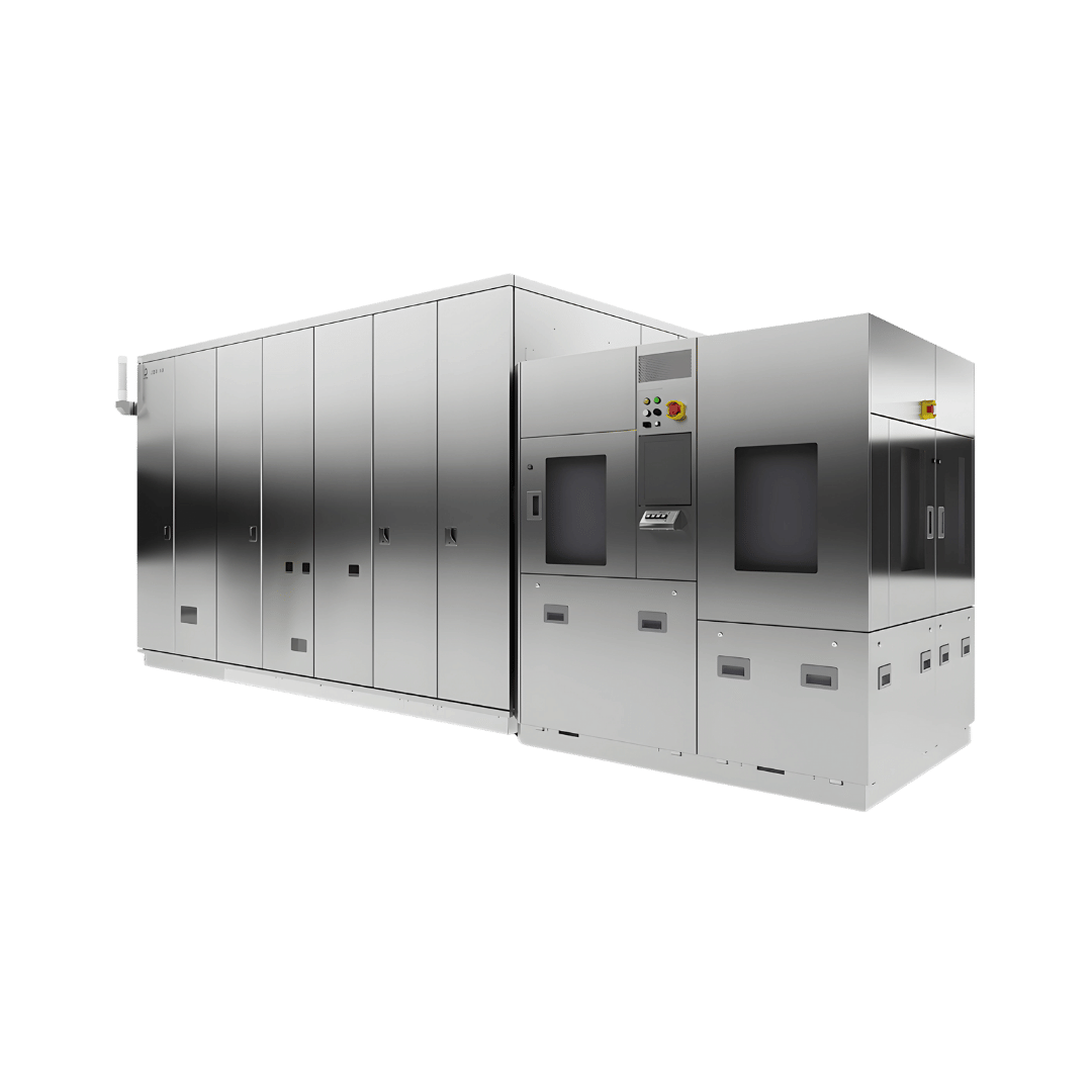
The JEOL JBX-A9 Series Electron Beam Lithography System is a state-of-the-art direct writing system designed for high precision and high throughput applications. Building upon JEOL’s advanced electron optics technology, the JBX-A9 offers exceptional stability and performance for semiconductor fabrication and nanofabrication processes.
Key Features:
High Precision and Throughput: The JBX-A9 is engineered to deliver both high precision and high throughput in electron beam lithography, making it suitable for advanced research and industrial applications.
Advanced Electron Optics: Incorporating JEOL’s renowned electron optics, the system ensures ultimate stability during operation, contributing to consistent and reliable patterning results.
Wafer Compatibility: The system accommodates wafers up to 300 mm in size, addressing the needs of modern semiconductor manufacturing processes.
FOUP Integration: An optional Front-Opening Unified Pod (FOUP) system is available, facilitating seamless integration into automated wafer handling environments and enhancing production efficiency.
In-Line Extendibility: The JBX-A9 offers in-line extendibility to other process tools, such as coaters and developers, enabling streamlined workflows and reduced processing times.
Energy Efficiency: Designed with low power consumption in mind, the system supports sustainable operation without compromising performance.
User-Friendly Interface: The system’s improved ease-of-use caters to operators of all experience levels, reducing the learning curve and promoting operational efficiency.
Technical Specifications:
Accelerating Voltage: 100 kV
Maximum Field Size: 1000 μm
Minimum Increment:25 nm
Stitching Accuracy: ±9 nm
Overlay Accuracy: ±9 nm
Minimum Line Width: ≤8 nm
Beam Current Range: 50 pA to 400 nA
Maximum Scanning Speed: 200 MHz
Stage Positioning Resolution:15 nm
Automatic Aberration Corrections: Includes dynamic focus, dynamic stigmatism, and deflection distortion correction
Maximum Sample Size: Supports 300 mm wafers and 9-inch masks
Power Consumption: 5 kVA
System Footprint:4 m × 5.3 m × 2.7 m (H)
Basic Configuration:
Main Unit: Includes the core lithography system
Auto Loading System: Features a 10-cassette auto-loading mechanism for efficient sample handling
Control Program: Equipped with a CPU system for precise control and operation
Data Preparation Program: Additional licenses available for comprehensive data preparation
Remote Control: Includes an OL aperture for remote operation capabilities
Optional Features:
In-Situ Optical Microscope: Allows for real-time observation and alignment during lithography processes
FOUP Wafer Auto Loading System: Enhances automation and integration within semiconductor fabrication environments
Open Cassette 200 mm Wafer Auto Loading System: Provides flexibility for handling different wafer sizes
48 kV High Voltage Program: Offers additional operational flexibility
SECS/GEM: Supports industry-standard communication protocols for equipment integration
Air Conditioner: Maintains optimal operating conditions
EMI Cancellation System: Reduces electromagnetic interference for enhanced performance
The JEOL JBX-A9 Series is a versatile and efficient electron beam lithography system, ideal for applications requiring high precision and throughput. Its advanced features and customizable options make it an asset for both research institutions and industrial manufacturers aiming to achieve cutting-edge results in nanofabrication and semiconductor device development.