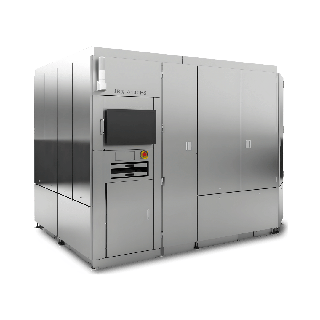
JBX-8100FS Series

Electron Beam Lithography System

The JEOL JBX-8100FS Series is a state-of-the-art Electron Beam Lithography (EBL) system designed to meet the demanding requirements of high-throughput and high-precision applications in nanofabrication and semiconductor device production. Leveraging JEOL’s advanced electron optics technology, the JBX-8100FS offers exceptional stability and performance for both research and industrial purposes.

Key Features:

  • Compact Design: The JBX-8100FS boasts a small footprint, with dimensions of 4.9 m (W) x 3.7 m (D) x 2.6 m (H), making it significantly more space-efficient compared to conventional systems.
  • Low Power Consumption: Designed with energy efficiency in mind, the system operates at approximately 3 kVA, reducing power usage to one-third of that required by traditional EBL systems.
  • High Throughput: Equipped with two exposure modes—high-resolution and high-throughput—the JBX-8100FS supports a variety of patterning needs, from ultra-fine processing to small to mid-size production. The system minimizes idle time during exposure and achieves a maximum scanning speed of 125 MHz, one of the highest levels globally, facilitating rapid and efficient writing processes.
  • Modular and Upgradeable Platform: The system is available in two versions: G1 (entry model) and G2 (full-option model). Optional accessories can be added to the G1 model as needed, allowing for customization based on specific application requirements.
  • Advanced Electron Optics: Incorporating JEOL’s renowned electron optics technology, the JBX-8100FS ensures ultimate stability during operation, contributing to consistent and reliable patterning results.
  • Versatile Substrate Compatibility: The system accommodates substrates up to 200 mm in diameter, 6-inch mask blanks, and small samples of various sizes, catering to diverse fabrication needs.
  • Enhanced Usability: The JBX-8100FS features a versatile Linux® operating system combined with a new graphical user interface, providing ease of operation. The data preparation program supports both Linux® and Windows®, enhancing flexibility for users.

Specifications

Version G1 (Entry model) G2 (Full option model) G3 (200kV model)
Writing method Spot beam, vector scan, step and repeat. Spot beam, vector scan, step and repeat. Spot beam, vector scan, step and repeat.
Acceleration voltage 100 kV 100 kV / 50 kV 200 kV / 130 kV / 100 kV / 50 kV
Beam current 5 × 10-12  to  2 × 10⁻⁷ A 5 × 10-12  to  2 × 10⁻⁷ A 5 × 10-12  to  2 × 10⁻⁷ A
Field size Maximum 1,000 μm × 1,000 μm Maximum 2,000 μm × 2,000 μm Maximum 2,000 μm × 2,000 μm
Scanning speed Maximum 125 MHz Maximum 125 MHz Maximum 125 MHz
Stage movable area 190 mm × 170 mm 190 mm × 170 mm 190 mm × 170 mm
Overlay accuracy ≦±9 nm ≦±9 nm ≦±8 nm
Stitching accuracy ≦±9 nm ≦±9 nm ≦±8 nm
Electric requirements (Normal) 3kVA 3kVA 3kVA
Substrate size Maximum 200mmΦ wafer Maximum 200mmΦ wafer Maximum 200mmΦ wafer
6 inch mask blanks 6 inch mask blanks 6 inch mask blanks
Small sample of any size Small sample of any size Small sample of any size
Substrate transfer Single auto loader 12 cassettes auto loader 12 cassettes auto loader
Major installable Options Optical microscope
25 kV high voltage program
Data preparation program additional license
High resolution laser beam control system


Optional Features:

  • Optical Microscope: An optional in-situ optical microscope is available, enabling real-time observation and alignment during lithography processes.
  • High-Voltage Program: A 25 kV high-voltage program is available as an option, offering additional operational flexibility.
  • Data Preparation Program: Additional licenses for the data preparation program can be acquired to enhance data processing capabilities.
  • High-Resolution Laser Beam Control System: An upgrade to a high-resolution laser beam control system is available, improving stage positioning resolution to 0.15 nm.

The JEOL JBX-8100FS Series is a versatile and efficient electron beam lithography system, ideal for applications requiring high precision and throughput. Its advanced features and customizable options make it a top choice for both research institutions and industrial manufacturers aiming to achieve cutting-edge results in nanofabrication and semiconductor device development.

For more detailed information about the JBX-8100FS Series, please visit the official JEOL website.

Skip to content